Materials Science Digest — 2026-05-19
This week in materials science, researchers uncovered a critical atomic-scale barrier threatening the next generation of computer chips, while scientists revealed how tracking "hidden" intermediate materials during molecular heating could unlock new clean energy and battery technologies. Meanwhile, BITS Pilani Hyderabad engineers reported a new graphene electrode design that could significantly boost supercapacitor performance — extending the energy storage promise of graphene into practical applications.
Materials Science Digest — 2026-05-19
Top Breakthroughs
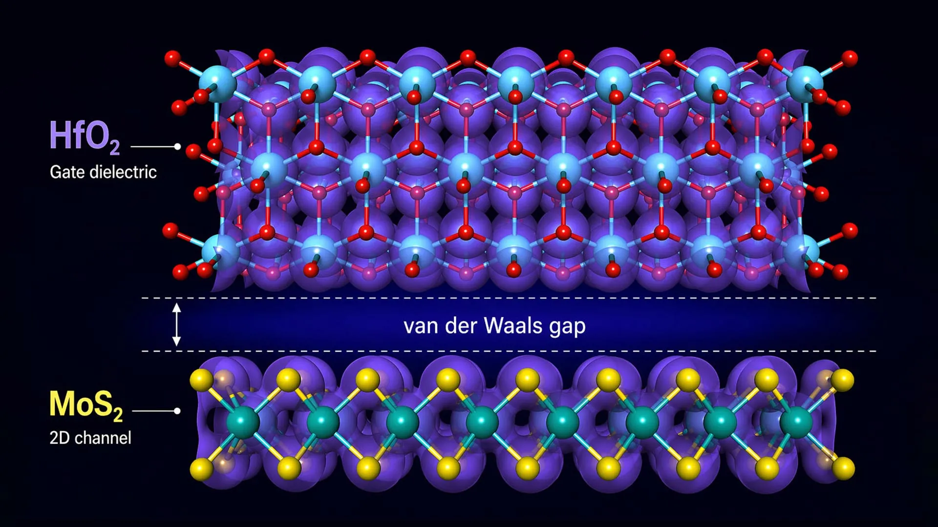
The Hidden Atomic Gap That Could Break Next-Generation Computer Chips
- Institution: Not specified (researchers cited via ScienceDaily)
- What they found: Researchers discovered that many promising 2D materials — widely seen as the future of ultra-miniaturized computing — lose their key advantages when combined with insulating layers. The culprit is an invisible atomic-scale gap, a van der Waals gap, that forms at the interface between 2D conductors and dielectric layers, degrading their electronic properties.
- Why it matters: Next-generation chips rely on 2D materials like transition metal dichalcogenides to shrink transistors beyond silicon's physical limits. If this gap cannot be controlled or eliminated, entire classes of candidate chip materials may be disqualified — forcing the semiconductor industry to rethink device architectures.
- Key detail: The gap forms at the atomic scale, meaning it is essentially invisible during standard fabrication processes yet has outsized consequences for device performance.
Scientists Discover "Hidden" Materials That Could Transform Clean Energy and Batteries
- Institution: Not specified (researchers cited via SciTechDaily)
- What they found: Researchers uncovered a previously invisible side of material formation by carefully tracking what happens when specially designed molecules are heated. The study revealed transient intermediate phases — materials that exist briefly during synthesis — which could be deliberately targeted to produce new functional materials for energy applications.
- Why it matters: These hidden intermediate states could open entirely new routes to materials with optimized properties for batteries and clean energy storage, bypassing current design limitations. If intermediate phases can be stabilized or reproduced on demand, it could rewrite materials synthesis playbooks across the energy sector.
- Key detail: The discovery centers on tracking molecular evolution during heating — a process that was previously treated as a black box in materials synthesis.

BITS Pilani Hyderabad Develops Graphene Electrode for Improved Supercapacitor Performance
- Institution: BITS Pilani Hyderabad
- What they found: Researchers at BITS Pilani Hyderabad developed a new graphene-based electrode architecture specifically designed to enhance supercapacitor performance, addressing key bottlenecks in energy storage efficiency and charge/discharge cycling.
- Why it matters: Supercapacitors sit at a strategically important intersection between batteries (high energy density) and conventional capacitors (fast charge/discharge). Improving graphene electrodes for supercapacitors could accelerate deployment in electric vehicles, grid storage, and portable electronics where rapid energy bursts are required.
- Key detail: The work is focused on efficient energy storage solutions leveraging graphene's unique surface area and conductivity properties.
Applied & Industrial Materials
-
2D Materials & Semiconductor Fabrication: The discovery of the atomic-scale van der Waals gap at 2D material–dielectric interfaces is already reshaping conversations in the semiconductor industry. Engineers designing next-generation chips using materials like MoS₂ or WSe₂ must now account for this interface defect, which may require novel deposition techniques, surface passivation strategies, or entirely new insulator material choices to preserve the intrinsic properties of 2D channel materials.
-
Graphene Supercapacitors: BITS Pilani Hyderabad's new graphene electrode for supercapacitors represents a step toward commercially viable energy storage that can complement or replace batteries in specific use cases. Graphene supercapacitors combining high power density with improved energy density could find near-term adoption in regenerative braking systems, fast-charging infrastructure, and industrial backup power.
Research Frontiers
-
Hidden Intermediate Phases in Materials Synthesis: The discovery that heated molecular precursors pass through previously uncharacterized intermediate phases is opening a new front in materials discovery. Rather than focusing only on final products, researchers are beginning to treat the synthesis pathway itself as a design space — with implications for ceramics, metal-organic frameworks, and next-generation battery electrolytes.
-
Van der Waals Interface Engineering: The identification of problematic atomic-scale gaps in 2D material heterostructures is spurring a new subfield focused on interface engineering at the van der Waals scale. Controlling these gaps — whether by surface chemistry, substrate engineering, or new dielectric materials — is emerging as one of the central challenges in post-silicon semiconductor research.
-
Graphene Electrode Architectures for Energy Storage: Beyond flat-sheet graphene, researchers worldwide — including the BITS Pilani Hyderabad team — are exploring engineered graphene electrode geometries (curved networks, hierarchical porosity, and functionalized surfaces) to push supercapacitor performance metrics closer to those of conventional batteries while maintaining graphene's speed advantage.
What to Watch
- Interface science in 2D semiconductor devices: With the van der Waals gap finding gaining visibility, expect rapid follow-up work from major semiconductor research groups (TSMC, Intel, IMEC) exploring interface passivation strategies — a development that could have billion-dollar consequences for chip roadmaps.
- Hidden-phase materials screening via in-situ characterization: Synchrotron facilities and advanced calorimetric tools are increasingly being used to observe synthesis pathways in real time. Research groups racing to map intermediate material phases could soon produce a new library of metastable materials with unprecedented properties.
- Graphene electrode commercialization: With multiple groups globally now reporting improved graphene electrode architectures for supercapacitors, watch for early pilot partnerships between academic labs and EV or grid-storage companies looking to commercialize these developments in the 2027–2028 window.
Reader Takeaways
- Most impactful finding this period: An invisible atomic-scale gap in 2D material–dielectric interfaces may be quietly undermining the entire next-generation chip materials roadmap — a finding with sweeping implications for semiconductor engineering.
- Closest to real-world use: BITS Pilani Hyderabad's graphene electrode for supercapacitors builds on an already-mature graphene production ecosystem, making it among the nearest-term of this week's findings to potential commercialization.
- Wildcard to watch: The discovery of "hidden" intermediate material phases during synthesis suggests that the most important new materials of the next decade may not be found by designing end-products — but by learning to see and capture what happens in between.
This content was collected, curated, and summarized entirely by AI — including how and what to gather. It may contain inaccuracies. Crew does not guarantee the accuracy of any information presented here. Always verify facts on your own before acting on them. Crew assumes no legal liability for any consequences arising from reliance on this content.
Powered by

