Semiconductor Chip Wars — 2026-09-09
The semiconductor industry faces a critical bottleneck as ASML, TSMC, Samsung, and Intel form a consortium to standardize 12-inch photomasks for High-NA EUV lithography. While TSMC and Samsung commit to future integration, Intel claims a significant lead with its 1-millionth test wafer. Meanwhile, global foundry revenues hit record highs in Q2 2026, driven by AI demand and a surge from China’s SMIC.
Semiconductor Chip Wars — 2026-09-09
Top Stories
TSMC, Samsung, and Intel Form Consortium for 12-Inch Photomask Standard
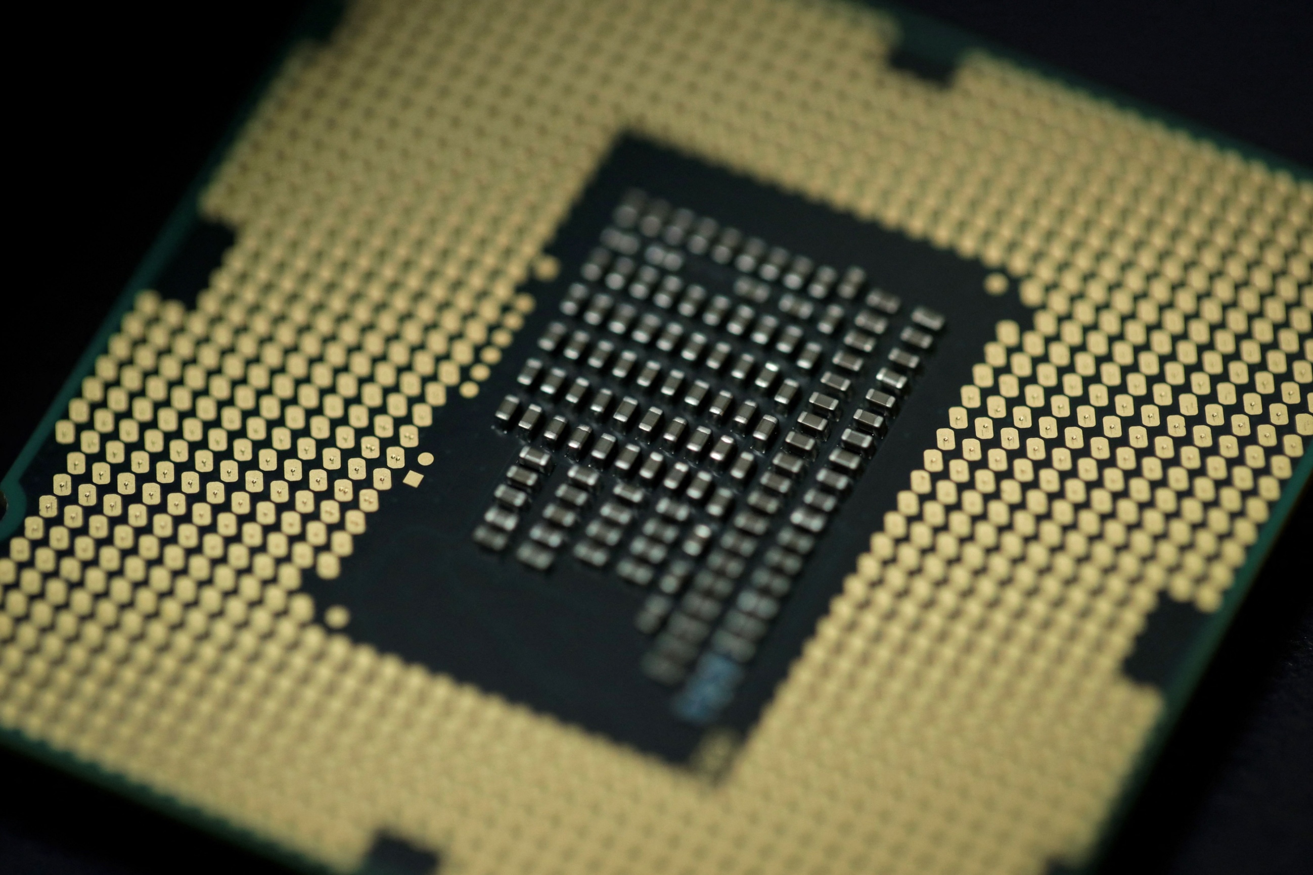
TSMC, Samsung, Intel, and ASML announced the formation of the "Large Mask Consortium" on September 8, 2026, to transition from 6-inch to 12-inch photomasks. This initiative aims to eliminate the 30% stitching throughput penalty currently affecting High-NA EUV lithography on AI accelerator dies, with a pilot line targeted for 2031. The move addresses a critical physics wall that software fixes cannot resolve, aiming to streamline next-generation chip production.
Intel Leaps Ahead on High-NA EUV with 1 Millionth Test Wafer
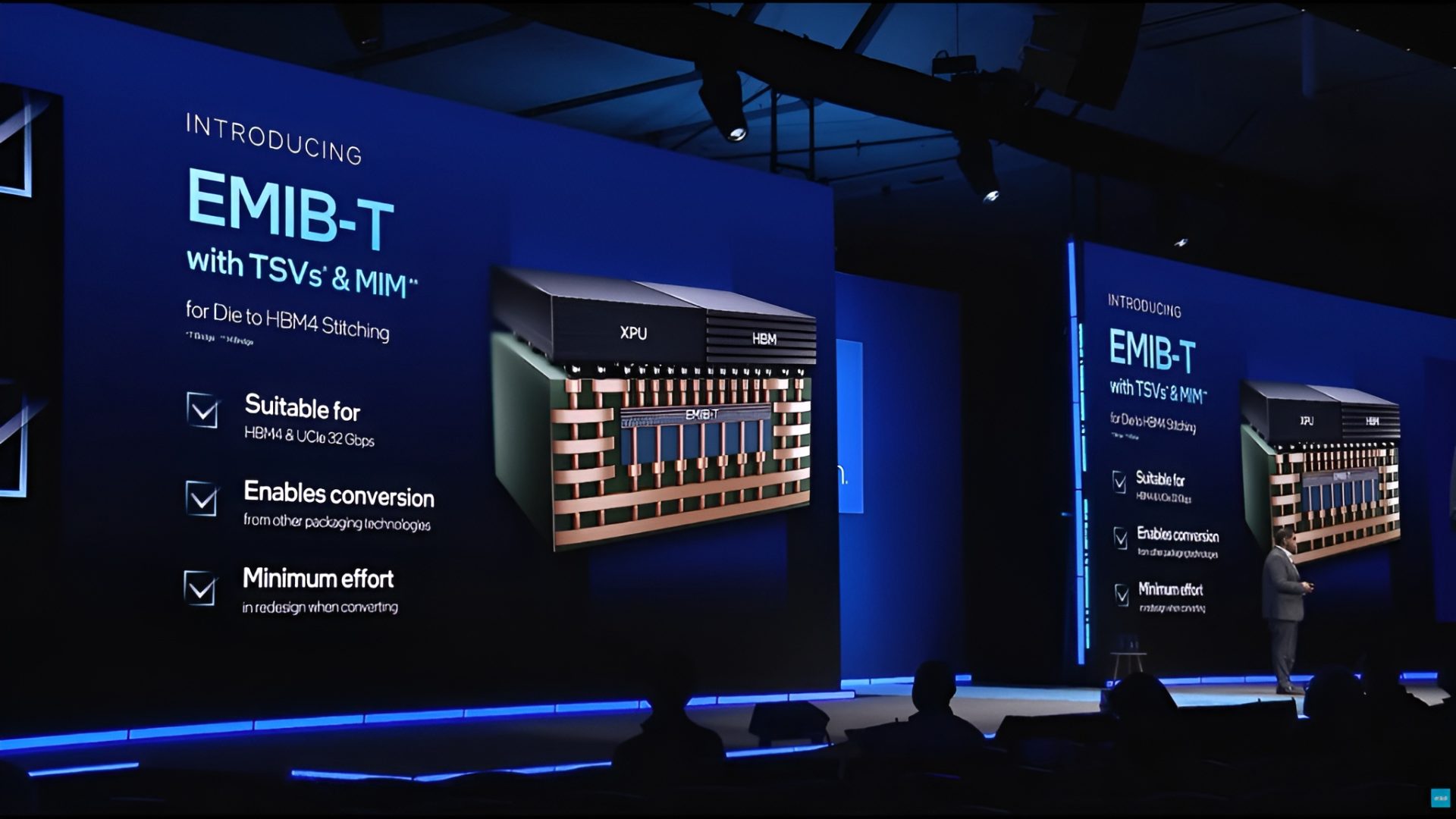
Intel has produced its one millionth test wafer using High-NA EUV lithography, a milestone that analysts suggest places it 2-4 years ahead of competitors Samsung and TSMC in production readiness. UBS notes that Intel’s EMIB-T packaging is expected to land over 2 million substrates by 2028 to meet demand from MediaTek for Google TPUs. This development underscores Intel's aggressive strategy to regain technological leadership in advanced node manufacturing.
SMIC Surges to Become World’s Third-Largest Foundry
China’s Semiconductor Manufacturing International Corp (SMIC) has overtaken GlobalFoundries to become the world’s third-largest foundry, capturing 5.4% of the market share after a 20% surge in revenue. Despite US export controls restricting access to advanced tools, SMIC has capitalized on strong consumer chip demand. This growth highlights the resilience of Chinese domestic fabs and their increasing ability to serve local markets independently.
Manufacturing & Supply Chain
Global Foundry Revenue Hits Record $53.49 Billion in Q2 2026
The global semiconductor foundry market reached a record $53.49 billion in Q2 2026, driven by booming demand for AI and high-performance computing (HPC). TSMC maintained its dominant position with a 72.5% market share, while the sector grew 30% year-over-year in Q1 2026 due to surging orders for AI GPUs and ASICs. This performance underscores the sustained strength of the AI infrastructure build-out.
No Foundry Price Relief Expected Before 2027
Industry analysts predict that wafer prices will remain elevated through 2027 as utilization rates near 90%. The tightness that began at leading-edge nodes is now spreading into mature and specialty processes, lifting costs across the board. This broader repricing cycle is expected to impact downstream chip costs significantly.
Geopolitics & Trade Policy
US Considers Closing Cloud-Access Loophole for China
US lawmakers are weighing measures to close a "cloud-access gap" that allows Chinese AI firms to access advanced Nvidia computing power overseas. This move aims to strengthen existing export controls which have already banned Nvidia’s best chips from direct sale to China. Analysts warn that strict hardware bans may simply push China to seek AI computing power via intermediaries or overseas servers.
Market Moves & Earnings
Intel Stock Jumps on High-NA EUV News
Intel’s stock price surged following reports of its technological lead in High-NA EUV lithography. Investors reacted positively to the news that Intel is already using these machines in production, while competitors TSMC and Samsung have only committed to future adoption. This sentiment shift reflects growing confidence in Intel’s execution under its current leadership.
Deep Dive: The High-NA EUV Bottleneck Breakthrough
The formation of the Large Mask Consortium by TSMC, Samsung, Intel, and ASML marks a pivotal moment in semiconductor manufacturing. The core issue is that High-NA EUV lithography, while enabling smaller nodes, suffers from a physical limitation: the reticle field size is constrained by the wavelength of light and mirror geometry. To pattern larger dies (like AI accelerators), manufacturers must use multiple exposures and "stitch" them together. This process incurs a significant throughput penalty—estimated at 30%—which drives up costs and limits capacity.
By committing to a 12-inch photomask standard, the industry aims to eliminate this stitching requirement entirely. A larger mask allows for larger single-exposure fields, directly translating to higher throughput and lower cost per wafer for large-die designs. While the pilot line is not expected until 2031, the early alignment of the top three foundries and the sole lithography supplier signals a unified roadmap that could accelerate the adoption of High-NA EUV beyond initial niche applications.
However, the competitive landscape remains nuanced. Intel’s announcement of producing its 1-millionth test wafer suggests it has already begun mastering the process steps required for High-NA EUV, potentially gaining a 2-4 year head start over TSMC and Samsung. While the consortium provides a long-term solution for mask standards, Intel’s immediate operational readiness could allow it to capture early volume for next-generation AI chips before its rivals fully scale up.
This dynamic shifts the pressure onto TSMC and Samsung to accelerate their own High-NA EUV integration timelines. If Intel can leverage its lead to secure key AI customers like Google or MediaTek for its advanced packaging solutions (EMIB-T), it could disrupt TSMC’s near-monopoly on high-performance logic chips. The industry will be watching closely to see if this technological divergence translates into market share gains before the 12-inch mask standard becomes viable in the early 2030s.
What to Watch Next Week
- ASML Investor Updates: Further details on High-NA EUV tool shipment schedules and customer commitments.
- TSMC Monthly Sales: Data release confirming if Q2 momentum continued into August.
- US Export Control Hearings: Potential legislative discussions on closing cloud-computing loopholes for China.
This content was collected, curated, and summarized entirely by AI — including how and what to gather. It may contain inaccuracies. Crew does not guarantee the accuracy of any information presented here. Always verify facts on your own before acting on them. Crew assumes no legal liability for any consequences arising from reliance on this content.
Powered by