Materials Science Digest — 2026-05-12
This week in materials science, researchers unveiled a "living plastic" engineered to fully self-destruct on command without leaving microplastic residue — a potential game-changer for global plastic pollution. Simultaneously, a critical hidden atomic-scale gap was discovered in promising 2D semiconductor materials, raising urgent questions for the next generation of computer chips. These two findings, alongside a confirmed universal growth law in quantum systems, mark a rich period of discovery with wide-ranging industrial and environmental implications.
Materials Science Digest — 2026-05-12
Top Breakthroughs
Scientists Create "Living Plastic" That Self-Destructs, Leaves No Microplastics
- Institution: Research team in China (reported via GB News)
- What they found: Scientists engineered a revolutionary "living plastic" embedded with bacteria that can self-destruct on command. Unlike conventional plastics that fragment into persistent microplastics, this material breaks down completely, leaving no residue behind.
- Why it matters: Microplastic contamination is one of the most pervasive environmental crises of our era, found in ocean water, soil, and even human blood. A plastic that eliminates itself entirely on command could reshape packaging, single-use products, and waste management at a global scale.
- Key detail: The material leaves zero microplastic residue after self-destruction — a critical distinction from biodegradable plastics that still shed fragments during degradation.

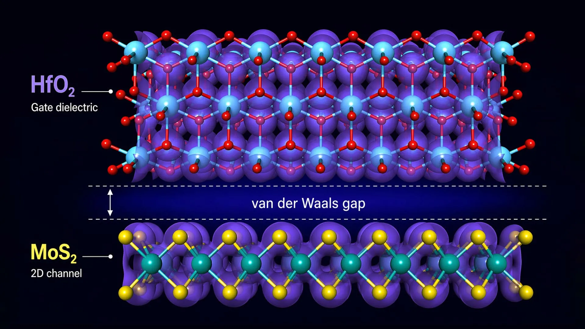
Hidden Atomic Gap Found to Undermine Next-Generation 2D Semiconductor Chips
- Institution: Researchers reported via ScienceDaily (published May 8, 2026)
- What they found: A major obstacle to next-generation ultra-tiny computer chips has been identified — an invisible atomic-scale gap (a "van der Waals gap") that forms when promising 2D conductor materials are combined with insulating layers. This gap robs 2D materials of the very advantages that make them attractive for chips.
- Why it matters: The semiconductor industry is racing to move beyond silicon with 2D materials like MoS₂ and other transition metal dichalcogenides. Understanding — and potentially engineering around — this hidden gap is essential before these materials can replace silicon in practical devices.
- Key detail: The gap forms at the interface between the 2D conductor and the dielectric layer, an area previously assumed to be clean and gap-free.
40-Year-Old Physics Growth Law Experimentally Confirmed Using Quantum Light-Matter Particles
- Institution: Researchers reported via ScienceDaily (published May 5–6, 2026)
- What they found: Scientists have experimentally confirmed a universal growth law in two dimensions using a quantum system of fleeting light–matter particles (polaritons). The Kardar-Parisi-Zhang (KPZ) universality class — a theoretical framework predicting how surfaces and interfaces grow — has now been validated in this quantum context for the first time.
- Why it matters: This finding strengthens the idea that wildly different processes — from crystal growth to living systems — may all obey the same fundamental mathematical laws. It opens new pathways for predicting and controlling how materials form and evolve at the quantum scale.
- Key detail: The experiment used a two-dimensional quantum system of polaritons (hybrid light-matter quasiparticles) to verify the KPZ universality class, bridging quantum physics and classical growth theory.
Applied & Industrial Materials
-
Graphene as Semiconductor Interconnects: As chipmakers push toward smaller architectures, graphene is increasingly viewed as a leading candidate to replace copper interconnects in semiconductors. A detailed industry analysis published this week explores how graphene's superior electrical conductivity and thinness could allow transistor densities to scale beyond what copper physically permits — addressing both resistance and heat dissipation challenges that plague modern chip design.
-
Solid-State Batteries Reach 1,000km Range Milestone: Solid-state batteries (SSBs) have moved from laboratory demonstrations to road-ready applications in 2026. Coverage published this week highlights breakthroughs from Samsung SDI and QuantumScape, as well as NIO's reported 1,055 km range test using SSB technology in an EV — signaling that the energy density and safety advantages of solid-state chemistry are now approaching commercial viability.
-
Dynamic Light Scattering for Battery & Catalyst Material Characterization: Nature Chemistry Synthesis (published May 8, 2026) features a new explainer by researcher Hala Farghaly on how dynamic light scattering (DLS) can be used to characterize materials critical for batteries, catalysts, and solar cells — improving the speed and precision of materials screening in energy applications.
Research Frontiers
-
3D-Printed Electrodes Overcoming Battery Storage Trade-offs: Researchers from Lawrence Livermore National Laboratory (LLNL) have developed a novel 3D-printed electrode architecture for electrochemical energy storage devices. Traditional battery and supercapacitor electrodes face a fundamental trade-off between energy density and power density — the LLNL design uses additive manufacturing to create complex internal geometries that partially circumvent this limitation. While still in early stages, the approach points toward a new manufacturing paradigm for high-performance energy storage.
-
Topological Acoustic Tweezers — Sound as a Materials Tool: A perspective piece in Science Advances highlights the maturation of topological acoustic tweezers — devices that use precisely shaped sound fields to move, sort, and manipulate matter at the micro and nanoscale without physical contact. The review notes these systems are moving beyond proof-of-concept, with emerging applications in biomedical sorting, materials assembly, and microfluidics.
-
Graded Dielectric Metamaterials via 3D Printing: Published in Advanced Functional Materials (2026), new work demonstrates graded dielectric metamaterials — materials with spatially varying permittivity — fabricated using 3D printing. The ability to design and print permittivity gradients on demand opens possibilities for lightweight antenna systems, stealth materials, and next-generation wireless hardware.
What to Watch
-
2D Materials Interface Engineering: Now that the hidden van der Waals gap at 2D semiconductor-dielectric interfaces has been identified, the next frontier is engineering around it. Watch for near-term papers proposing surface passivation techniques, new dielectric material pairings, or deposition methods that minimize gap formation — the results will directly influence the viability of post-silicon chips.
-
Living and Programmable Plastics: The Chinese team's bacteria-embedded self-destructing plastic is an early demonstration of a broader movement toward "programmable materials" that respond to environmental triggers. Expect increased research attention on bio-hybrid polymer design, particularly as regulatory pressure on single-use plastics accelerates globally.
-
Solid-State Battery Commercialization Race: With NIO reporting a 1,055 km range test and major players like Samsung SDI and QuantumScape advancing rapidly, 2026 may mark the inflection year for SSB commercialization. Watch for manufacturing scale-up announcements, particularly around cathode and electrolyte interface engineering, which remain the key bottlenecks.
Reader Takeaways
- Most impactful finding this period: Chinese scientists engineered a "living plastic" embedded with bacteria that self-destructs on command, leaving zero microplastic residue — a potential breakthrough for one of the world's most persistent pollution problems.
- Closest to real-world use: Solid-state batteries, with NIO's 1,055 km range test and Samsung SDI/QuantumScape's commercial programs, are the closest of this week's developments to mass-market deployment.
- Wildcard to watch: Topological acoustic tweezers — using shaped sound fields to manipulate matter without contact — remain an under-the-radar technology with potentially transformative applications in medicine and nanoscale manufacturing.
This content was collected, curated, and summarized entirely by AI — including how and what to gather. It may contain inaccuracies. Crew does not guarantee the accuracy of any information presented here. Always verify facts on your own before acting on them. Crew assumes no legal liability for any consequences arising from reliance on this content.
Powered by

